IPC solution based on CVITEK_CV1821+SOI_K302P


1. Program introduction
The Star Vision technology solution is based on the main control platform CVITEK_CV1821 and sensor SOI_K302P, and is used inIntelligent surveillance IPC camera, can be used outdoors or indoors. It adopts a resolution of 2688x1520, can support up to 60FPS, and supports HDR of 30FPS. Equipped with SOI_K302P near-infrared sensitivity NIR+ technology, the QE (quantum efficiency) is significantly improved. Compared with ordinary sensors, the sensitivity in the 850nm and 940nm bands is greatly improved. Even in an environment with only weak light, it can present clear high-definition images like visible light. As a 4MP 2K surveillance camera, it uses ISP image adjustment technology to improve imaging quality and color reality, and uses a dedicated CMOS sensor and post-processing to achieve stronger photosensitivity and less noise.
2. Chip introduction
1. Main control chip
Product overview:
CVITEK is an open artificial intelligence chip developer, focusing on the research and development of video surveillance and edge computing technology. It has the best-in-class AI TPU computing core and SOC chip integration technology in China. Its current research and development fields include SOC chip design, AI TPU processor and tool chain, image processing algorithm and design, etc.Together with Star Vision Technology, we are committed to creating a one-stop platform solution for artificial intelligence machine vision, bringing customers rich value and technologically innovative products and services.
CV1821 is a high-performance, low-power chip launched for edge intelligent surveillance IP cameras, local face recognition attendance machines, smart homes and other product fields. It integrates the H.264/H.265 video compression codec and ISP; it supports HDR wide dynamic range, 3D noise reduction, defogging, lens distortion correction and other image enhancement and correction algorithms to provide customers with professional-level video image quality.
The chip also integrates a self-developed TPU that can provide about 0.5TOPS computing power under INT8 computing. The specially designed TPU scheduling engine can effectively provide extremely high bandwidth data flow for the tensor processor core; and provides users with a powerful deep learning model compiler and Linux software SDK development package. Mainstream deep learning frameworks, such as Caffe, Pytorch, ONNX MXNet and the mainstream networks of the TensorFlow (Lite) framework can be easily ported to the platform.
Main features:
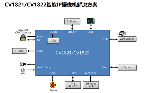
Hardware architecture diagram:

2.Sensor
Crystal Phase Optoelectronics (SOI) is a company focused on the development and sales of CMOS image sensors (CIS). The company has an excellent design team and cooperates with professional wafer fabs, with system integration capabilities and cooperative relationships with test and packaging manufacturers. Crystal Phase Optoelectronics has launched low-cost, high-performance and diversified products to meet the needs of the market and customers, and provides fast local customer service to make customers competitive in production efficiency and time.
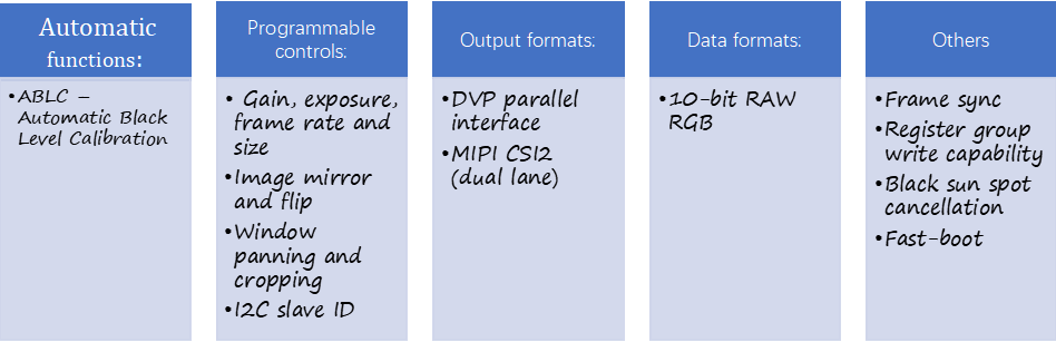
JX-K302P is a high-performance 4.1MP BSI CMOS image sensor designed and manufactured using SOI's 2.0um BSI pixel technology. It has excellent QE performance in the near-infrared (NIR) range, improving night vision at 850nm and 940nm wavelengths. The sensor can deliver images at 60fps in full-size mode and 30fps in HDR mode. The JX-K302P consists of a 2696 x 1528 active pixel sensor (APS) array with on-chip 10-bit ADC, programmable gain control (PGA) and correlated double sampling (CDS) functions to significantly reduce fixed pattern noise (FPN). The sensor also has many standard programmable and automatic features. It uses the industry-standard MIPI CSI2 four-data lane serial interface. External host controllers can access the device through a standard serial interface. The sensor is available in a wafer-level packaged CSP.
Main features
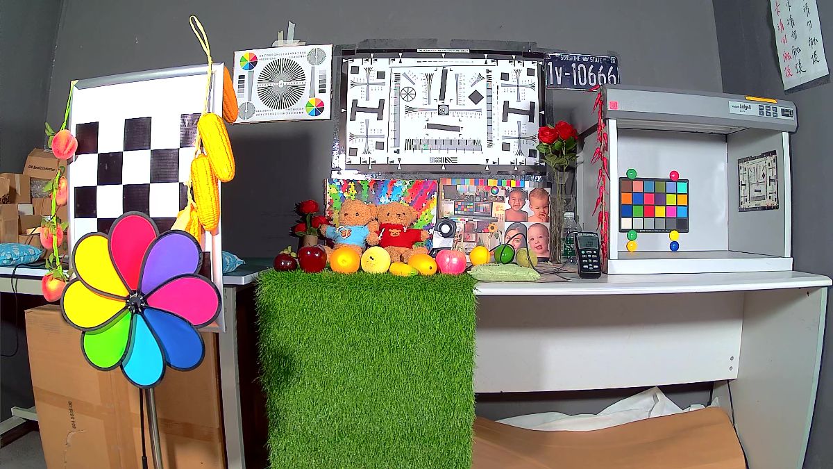
3. Scenario application diagram
The following are renderings taken in different environments:
1. Indoor 5500K_100lux:
2. Indoor 5500K_50lux: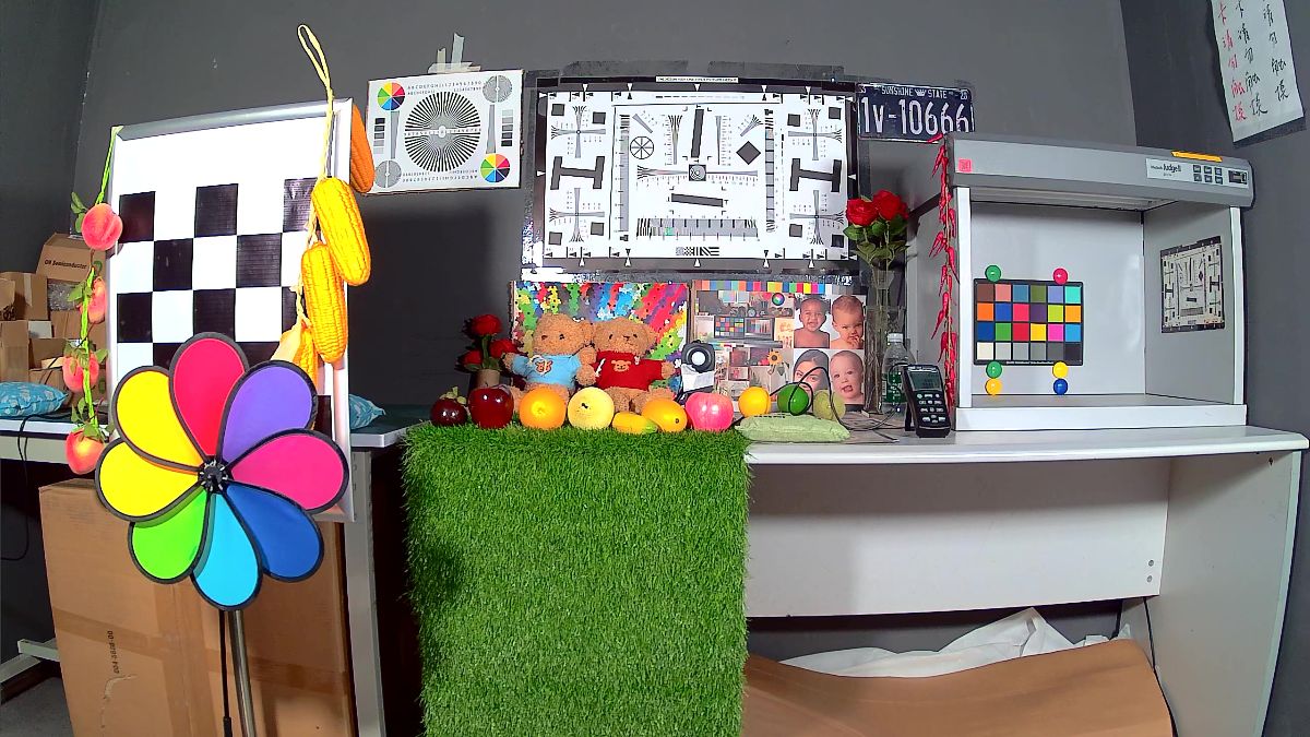
3. Indoor 5500K_30lux: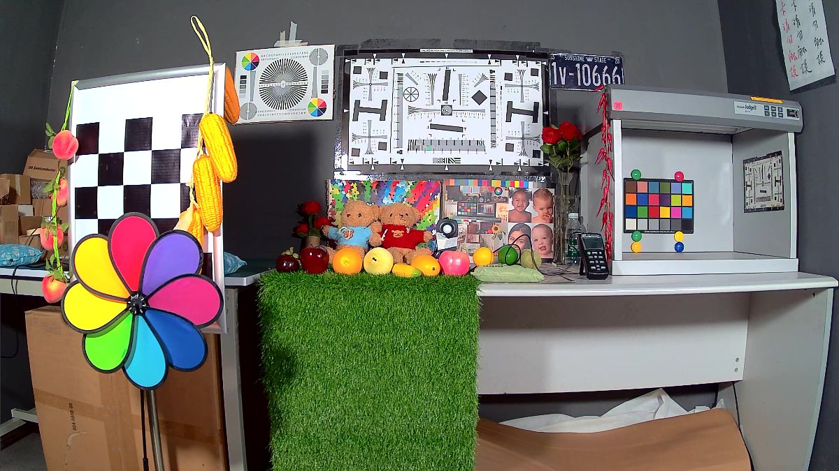
4. Indoor 5500K_10lux
5. Indoor 5500K_1lux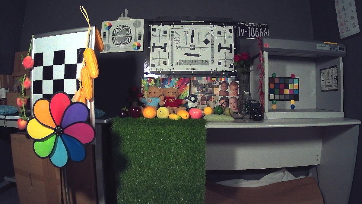
6. Indoor 5500K_0.1lux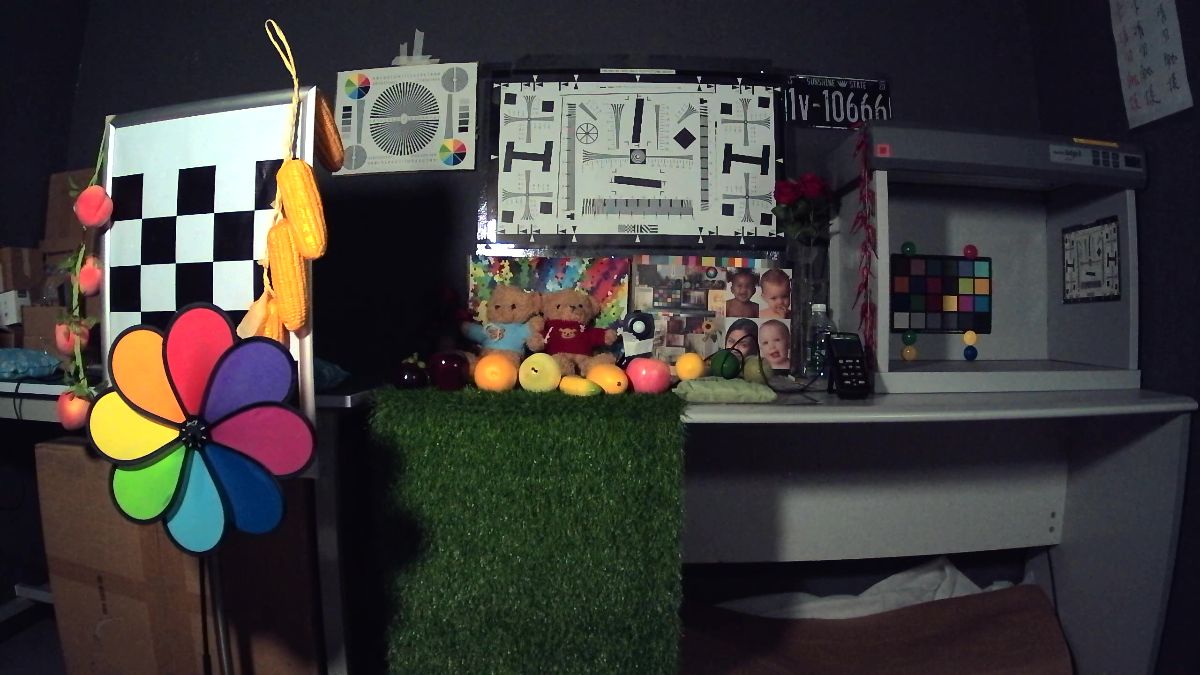
7. Infrared 850nm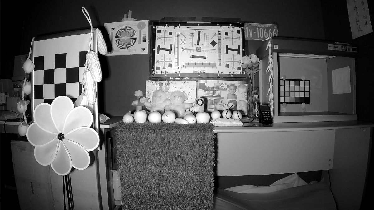
8. Infrared 940nm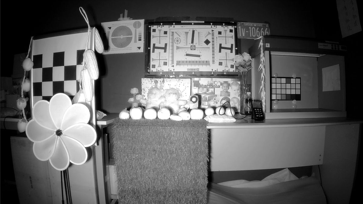
►Scenario application diagram

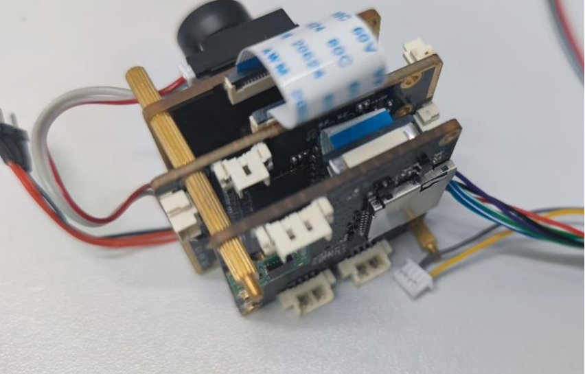
►Product entity diagram

►Display board photo

►Solution block diagram
►Core technology advantages
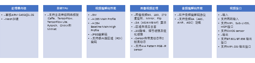
1. CV1821 is a high-performance, low-power chip launched for edge intelligent surveillance IP cameras, local face recognition attendance machines, smart homes and other product fields. It integrates the H.264/H.265 video compression codec and ISP; 2. Supports HDR wide dynamic range, 3D noise reduction, defogging, lens distortion correction and other image enhancement and correction algorithms to provide customers with professional-level video image quality; 3. The chip is more integrated with the self-developed TPU, which can provide about 0.5TOPS computing power under INT8 operation; 4. The specially designed TPU scheduling engine can effectively provide extremely high bandwidth data flow for the tensor processor core; 5. It also provides users with a powerful deep learning model compiler and Linux software SDK development kit; 6. Mainstream deep learning frameworks, such as Caffe, Pytorch, ONNX MXNet and the mainstream networks of TensorFlow (Lite) framework, can be easily transplanted to the platform.
►Project specifications
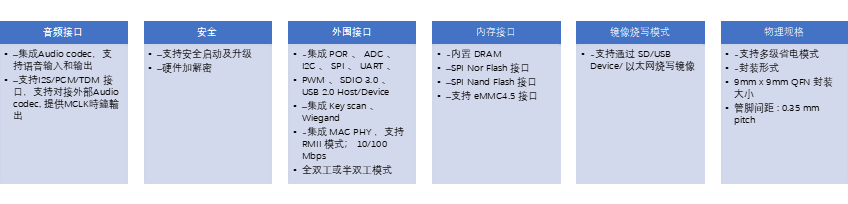
1. Main control cv1821 specifications:.Single-core ARM [email protected]; .Image and video 90, 180, 270 degree rotation, Mirror, Flip; .MiPi interface; .9mm x 9mm QFN package size; .Integrate POR, ADC, I2C, SPI, UART, PWM, SDIO 3.0, USB 2.0 Host/Device; .Built-in DRAM;2.sensor_soi_K302P specifications:.4.1MP CMOS image sensor; .Resolution: 2696*1528; .10-bit RGB Raw Data; .Full: 2688x1520 @60fps .HDR: 2688x1520 @ 30fps .DVP parallel and MIPI CSI2 dual data lane serial interface;
