

For the high-speed transmission rate of the USB family, how to improve the transmission quality of USB signals and reduce electromagnetic interference (EMI) and electrostatic discharge (ESD) has become the key to USB design. The following takes USB2.0 as an example to analyze from two aspects: circuit design and PCB design.
Electromagnetic compatibility design
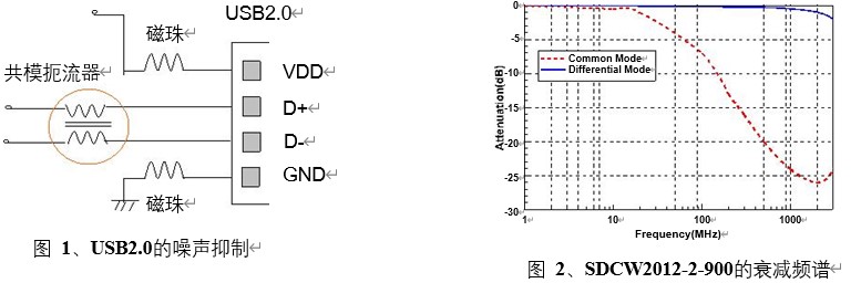
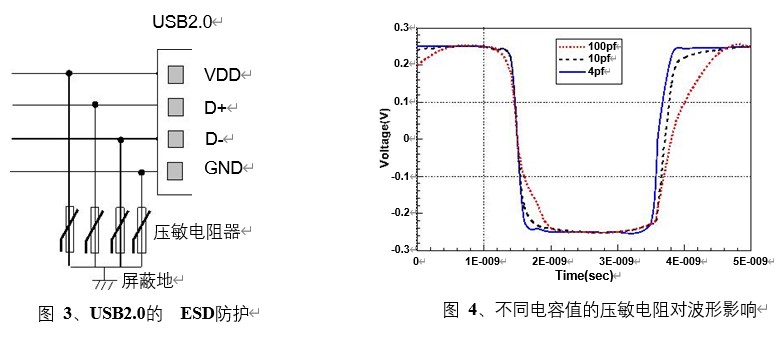
Under high-speed differential signal transmission in the USB2.0 interface, the radiated noise increases due to the signal swing between the ground layer and the power layer. Therefore, in order to avoid crosstalk and ensure the integrity of signal data, removing common mode noise that will be mixed into high-speed transmission signals is a necessary countermeasure for electromagnetic compatibility design. As shown in Figure 1, a magnetic bead PZ2012U121-2R0 with an impedance of 120 ohms and a rated current of 2A is connected in series to the data power line and the ground line respectively, and a common mode choke (Common Mode Choke Coil) SDCW2012-2-900 with a common mode impedance of 90 ohms is connected in series to the differential line pair. The common mode choke consists of two wires wound around the core material in the same direction. When the common mode current passes through, a high impedance will be generated due to the superposition of magnetic flux. For the differential mode current, the magnetic fluxes will cancel each other out, resulting in a smaller impedance. Taking SDCW2012-2-900 as an example, the differential mode impedance at 100MHz is only 4.6 ohms. From the attenuation characteristics in Figure 2, it can also be seen that the common mode choke will not affect the differential signal, and it is mainly used to selectively attenuate the common mode current.
ESD protection design
The harm of electrostatic discharge is everywhere, and because the USB interface is hot-swappable, it is easy to cause electrostatic damage to devices due to unavoidable human factors, such as crashes and board burnouts. Users who use USB interfaces urgently require the addition of anti-ESD protection devices. As shown in Figure 3, when DESD5V0U1BL ESD protection is not added, the data power line and ground wire are each connected to a varistor SDV1005A5R5C101NPT with an operating voltage of 5.5V and a capacitance of 100pF to the shielded ground. Because the data transmission speed is as high as 480Mbps, the differential line pair requires a device with an input capacitance of less than 4pF. A larger capacitor can deteriorate the data signal waveform and even cause bit errors. Therefore, the connected varistor has an operating voltage of 18V and a maximum capacitance of 4pF, SDV1005H180C4R0GPT.
The voltage waveform in Figure 4 also verifies that the varistor with a 4pF capacitance has little effect on the deformation of the waveform.
PCB layout design
For USB2.0 PCB layout, the following principles must be taken into account:1. Differential line pairs must maintain line length matching, otherwise it will affect timing offset, reduce signal quality, and increase EMI;
2. Keep the spacing between differential line pairs less than 10mm, and increase the spacing with other signal traces;
3. Differential wiring is required to be on the same board layer. Differences such as impedance and vias produced by different layers will destroy the effect of differential mode transmission and introduce common mode noise;
4. The coupling between differential signal lines will affect the external impedance of the signal line, and terminal resistors must be used to achieve maximum matching of the differential transmission lines;
5. Minimize via holes and other factors that can cause circuit discontinuity;
6. Avoid 90° traces that cause resistance discontinuity and use arcs or 45° broken lines instead;
7. The ground terminal of the varistor is connected to the shielding ground layer and placed at the port position.
